Design Guidelines: Basic Conductors
Patterning - All circuit designs contain critical dimensions necessary for compliance and performance. It is important to consider these when designing the circuit to not add unnecessary cost to the design. Conductor tolerances of <0.001" require more costly tooling to ensure compliance.
Basic Conductor Standard Layout Guidelines
|
|
.003"
|
Per side 20% Minimum Taper |
|
|
.005"
|
Per side 20% Minimum Taper |
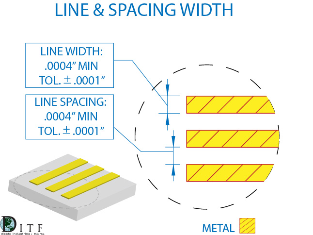
Line Spacing
|
.0004 minimum ± .0001"
|
Minimum space widths are a function of conductor thickness |
Line Width
|
.0004 minimum ± .0001"
|
Minimum line widths are a function of conductor thickness |
|
|
.001" minimum
|
.003" preferred |
|
|
.007" ± .005"
|
.006" typical radius, length 2 x material thickness |
|
|
.005" minimum +25%/-50%
|
increase or decrease of design area |
|
|
± .003"
|
± .001" by request |
|
|
0 - .003"
|
|
Multi Layer Conductor Standard Layout Guidelines
|
|
.003" Diameter
|
Ground signal ground up to 2 levels
|
|
|
.002" width .004" pitch
|
Ground signal ground up to 2 levels
|
|
|
.005"
|
|