Design Guidelines: Solder Masks
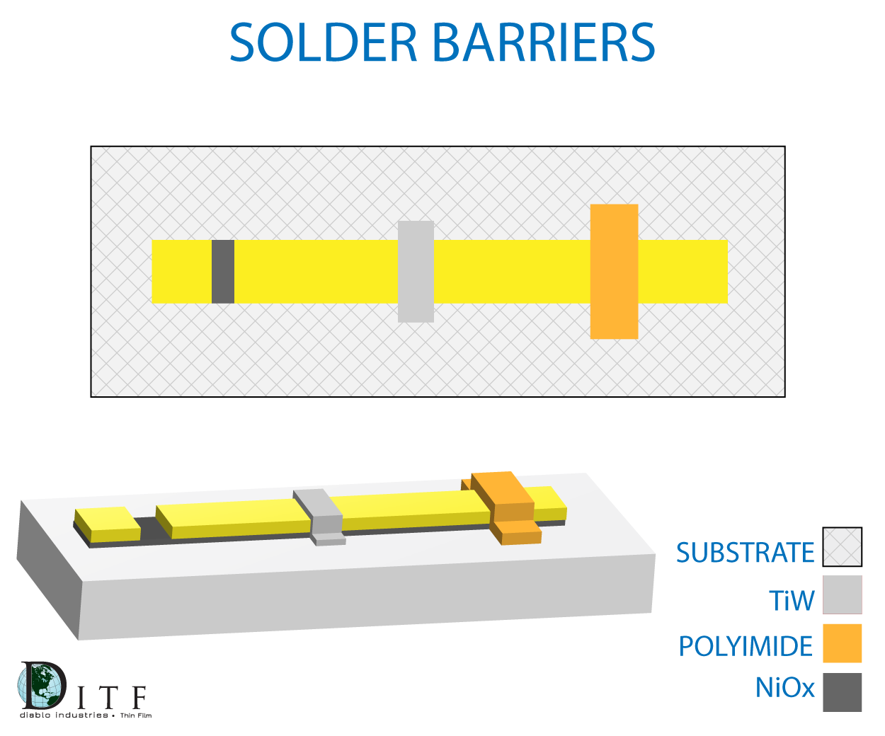
Various methods are available to provide the appropriate solder barrier, enhancing the ease of assembly of the design. Consult the factory for the optimum method for your design.
1. TiW - Knowles Precision Devices can provide a patterned TiW layer on the conductor surface to inhibit solder flow. This method is optimum for fast, lower temperature solders to restrict run out during reflow.
2. Polyimide - We provide patterned polyimide as a robust solder flow restrictor. With a thickness of 7um, polyimide can withstand higher temperature solders and provides a good, robust barrier to solder flow.
3. Nickel Oxide - Using our in house plating capability, a Nickel Oxide (NiOx) barrier is created by etching the top surface of gold exposing an underlying layer of Nickel and intentionally oxidizing the Nickel. The result is an extremely rubust solder flow restrictor. Note that this method requires an additional conductor layer below the Nickel layer.
|
Parameter
|
Material
|
|
TiW
|
Polyimide
|
NiOx
|
Comments
|
|
Thickness
|
1000 Â
|
160 - 320µ"
|
*20 - 300µ"
|
* Plated Nickel thickness |
|
Max. temperature
|
350°C/60 sec
|
425°C/60 sec
|
*N/A
|
* limited only by metallization scheme |
|
Min. gap width
|
.002"
|
.004"
|
.001"
|
|
|
Min. conductor overlap
|
.002"
|
.004"
|
*N/A
|
|
|
Min. feature width
|
.002"
|
.004"
|
*
|
* Width is equal to conductor width |
|
Distance to circuit edge
|
.003"
|
.003"
|
*N/A
|
* See metal feature to edge criteria |
|
Additive or Subtractive Process
|
Additive
|
Additive
|
Subtractive
|
|
|
Application side
|
A side, B side or both
|
|
Overall capability
|
Good
|
Better
|
Best
|
Based on user feedback |