Design Guidelines: Pre-deposited Solders
Knowles Precision Devices offers pre-deposited and patterned AuSn solder. On designs with multiple solder hierarchy or multiple pre-form sites, this can be a cost effective way to eliminate pre-forms. Consult the factory for available thicknesses and other details for applications and design criteria.
Note: The Au/Sn eutectic is a sputtered material (Au,80.4/ Sn,19.52 - Weight %, Typ); which provides superior flatness and thickness control. Typically, sputtered films can replace preforms of 2-3 times the thickness. Sizing of Au/Sn pads is critical and is developed from customer supplied information with respect to die size and tolerance .
Other solders are available on request, please contact our sales team for details
|
Parameter
|
Value
|
Units
|
|
Composition
|
80 Au / 20 Sn
|
Wt %
|
|
Melting Temeprature
|
284.0
|
°C
|
|
Density
|
14.5
|
g/cm3
|
|
Electric Conductivity
|
7.7
|
%IACS
|
|
Thermal Conductivity
|
57.0
|
W/mk
|
|
Temperature Coefficient of Expansion
|
16.0
|
m/mK
|
|
Resistivity
|
160.0
|
n ohm m
|
|
Modules of Elasticity
|
59.0
|
GPa
|
|
Tensile Strength
|
276.0
|
MPa
|
|
Feature
|
Value
|
Tolerance±
|
Comments
|
|
Thickness range
|
80 - 200 µ"
|
20 µ"
|
Most common thickness = 160 µ"
|
|
Minimum feature size
|
.005"
|
N/A
|
|
|
Solder pad pullback from Au metallization
|
.0015"
|
N/A
|
Eutectic pad is inboard of conductor
|
|
Au metallization pullback from substrate edge
|
.002"
|
N/A
|
Termination at edge is available, consult factory
|
|
Solder pad placement
|
N/A
|
.001"
|
|
|
Minumum substrate thickness
|
.005"
|
N/A
|
|
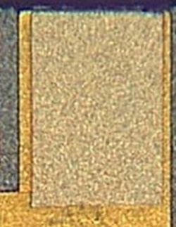
| gold / tin before reflow |
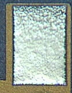
gold / tin after reflow |
 |
 |
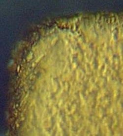
| gold / tin before reflow (close up) |
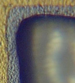
gold / tin after reflow (close up) |
 |
 |